Blog
Home » Diamonds blog » GROWTH OF THE LAB-GROWN DIAMOND SECTOR ANCHORED BY DEMAND FROM ELECTRONICS INDUSTRY
Focus on

Photo: Adi Gold on Unsplash.com.
While the laboratory-grown diamond market continues to grow at a rapid pace, it would be disingenuous to claim that its success is based on it being able to capture market share from natural diamonds. This is because the viability of manufactured diamonds as a product category is not altogether dependent on their being set in jewelry, or for that matter even for them being used predominately in that respect.
Indeed, the attractiveness of the laboratory-grown diamond industry as an investment vehicle quite possibly has less to do with jewelry than it has with electronics. And it’s not only a question of applicability, but also of total market value. Consider that the global diamond market size was valued at $94.96 billion in 2021, and is projected to reach $139.91 billion by 2030, increasing at a compound annual growth rate of 4.4 percent. Now consider that the global semiconductor market stood at an estimated $573.44 billion in 2022, and is forecast to grow to $1.38 trillion billion by 2029, at a CAGR of 12.2 percent.
In principle, diamonds have better ultra-wide bandgap semiconductor properties than silicon, and this at a time electronic engineers fear that they are reaching the physical limits of silicon for semiconductors.
As a semiconductor a lab-grown diamond can run five times hotter than silicon hotter without degrading in performance. It is also more easily cooled, with 22 times the heat transfer efficiency of silicon. This means diamonds tolerate higher voltages before breaking down, with electrons moving faster through them.
Driving that expansion will be new technologies, which require faster and more efficient semiconductors, including artificial intelligence, quantum computing, the Internet of Things, driverless automobiles and the metaverse. Diamonds, and more specifically lab-grown diamonds, are likely fill part of that demand.

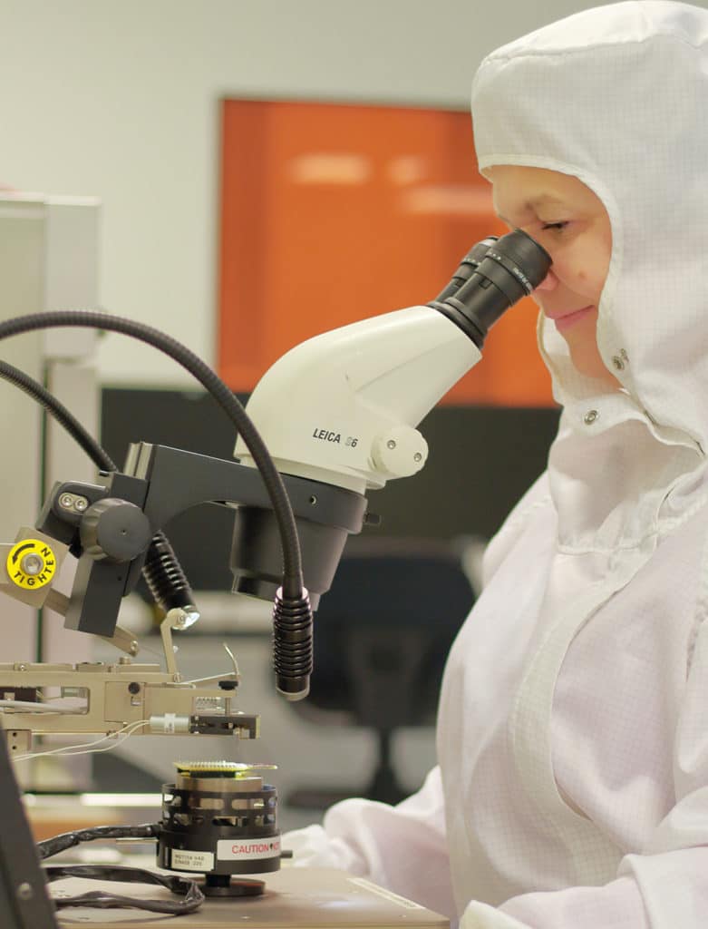
An engineer working on a semiconductor chip. (Photo: LN on Unsplash.com.
SMALLER, COOLER, FASTER, MORE POWERFUL
Silicon has been the popular material choice for semiconductors since the 1960s, and it still makes up 95 percent of the device types available in the market. But it presents several long-term challenges, with heat management among the most prominent.
When temperature rise above 150 degrees Celsius, silicon’s properties change and are no longer optimal. But a diamond can easily rise to 300 degrees Celsius. Thus, where a silicon converter requires a complex cooling system, diamond offers simpler and easier solutions.
The electronic industry today requires a silicon alternative that enabled devices to be smaller, cooler, faster, more powerful, and cleaner.
For power electronics, diamonds provide a tantalizing possibility material. They are thermally conductive, which means diamond-based devices would dissipate heat quickly and easily, foregoing the need for bulky and expensive methods for cooling. Diamond also handle high voltages and power, with electrical currents also flow through them quickly. They are suitable make for energy efficient devices.
Diamond-based semiconductors are capable of increasing power density, improving thermal performance within a device. Diamond films, which are about one-seventieth the diameter of a human hair, are able to form device structures that are over a thousand times thinner than the leading silicon counterpart.
PARTNERSHIP DRIVING DEVELOPMENT
To no small degree, the potential of the electronics sectors has been driving development in the lab-grown diamond sector. Among the key players is a research partnership involving the University of Bristol in the United Kingdom and Element Six, the largest lab-grown diamond division in the De Beers Group.
De Beers has been in the synthetic diamond business for about 70 years. Already in the 1950s, it established a project with the University of Bristol’s School of Physics, led by Sir Charles Frank, to better understand the features of natural diamonds and then to artificially imitate them through the application of heat and pressure, or as it became known, high-pressure, high-temperature (HPHT) processing.
When the new chemical vapor deposition (CVD) diamond-growing method, pioneered by Element Six, was developed, it was supported by a collaboration with the university’s Professor Mike to explore new opportunities, from high power density electronics to water treatment and quantum devices. Element Six which was created as an independent subsidiary from De Beers Industrial Diamond Division in 2002.
Element Six is now working with Martin Kuball, a professor of physics at the University of Bristol, to examine the diamond’s thermal conductivity. This has resulted in the creation and improvement of CVD diamond thermal solutions, enabling the ever-increasing power density necessary to satisfy the tremendous demand for new technologies.

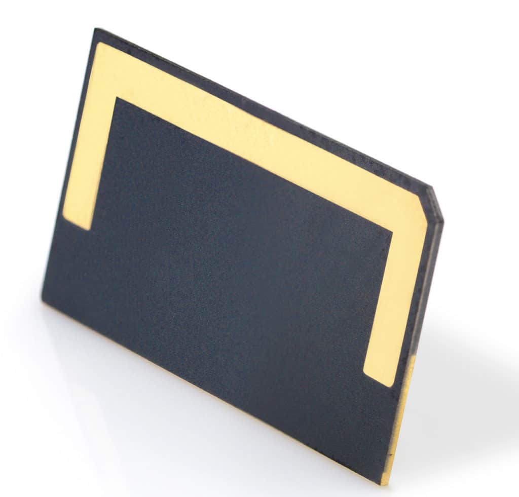
Diafilm, a customized CVD diamond semiconductor solution developed by Element Six, which enables system size reduction, improved reliability and the opportunity to design higher power systems.
